Zoom to Nano-resolution of Brain with New Imaging Tool

With the human brain being the most complex machine out there, a lot remains unexplained about it. Scientists insist that the known data of the human brain, is less than the unknown. But this imaging tool has enabled scientists to look into the brain in extreme close-up, and has made it possible to look into each cellular and even sub-cellular component clearly. This would greatly help with the better understanding of how signals travel in out brain (dendrites to axons to neuron) and other processes that not much focus has been given on.
WeissCollage

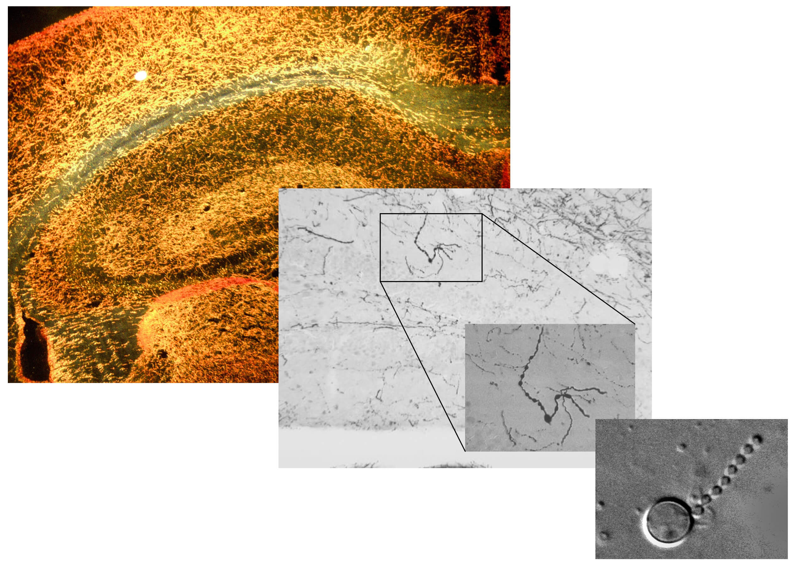
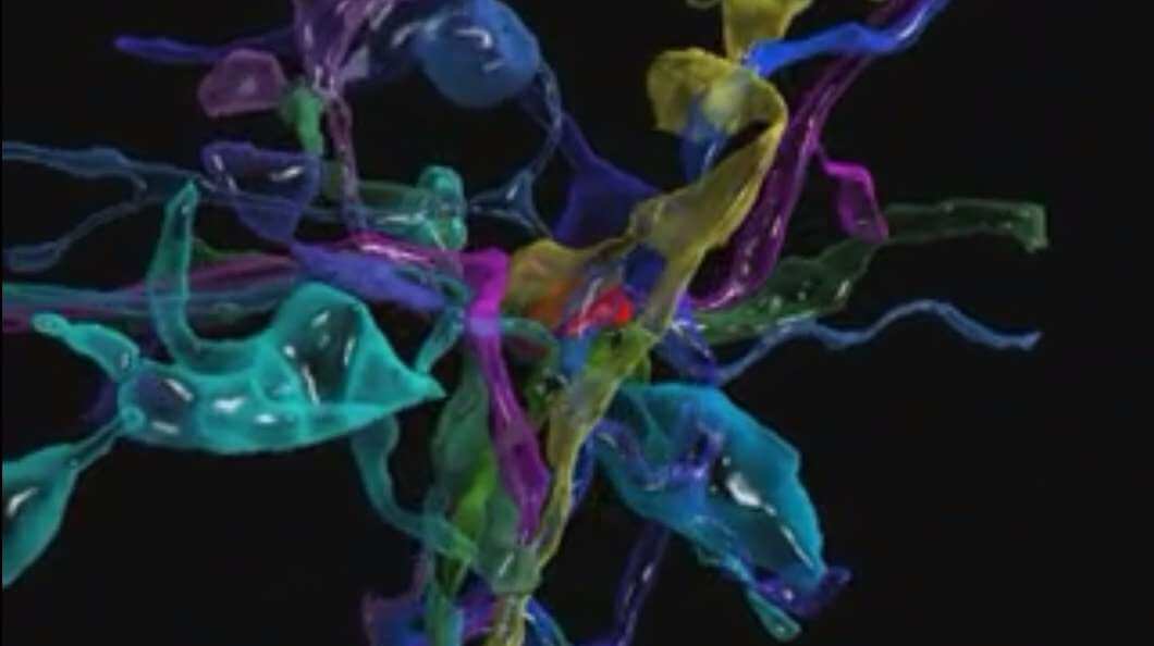
Researchers at the Boston University School of Medicine and Harvard University developed this imaging method which employs an automated tape-collecting device equipped with a diamond knife to obtain ultra-thin brain sections, which are then scanned under an electron microscope. Varied colours are allotted to different cellular components by a software generated by study co-author Daniel Berger.

The first test subject was an adult mouse. The sensory region associated with the mousse’s whiskers was studied. The neocortex of the mouse was zoomed into. The imaging tool allowed to see in clear detail, the synaptic clefts (space between neighbouring axon and dendrite). The neurotransmitter containing bag, called vesicles, were less than 40 nm in diameter. The sensitivity of the mouse’s whiskers proved to be more than those found in human fingertips!

Peter’s rule says that the connectivity between axons and dendrites could be inferred from their locations. This hypothesis has never been proved or disproved, even though the man responsible for it opposes it. The imaging tool has at last provided proof for the falsity of this hypothesis. Axons are of many types and may have one or even, three dendrites, which might have multiple synapses, instead of just one.
brain-imaging-tool-nanoscale-resolution@2x

Narayanan “Bobby” Kasthuri, study’s first author, says “We had this clean idea of how there’s a really nice order to how neurons connect with each other,” he explains, “but if you actually look at the material it’s not like that. The connections are so messy that it’s hard to imagine a plan to it. But we checked, and there’s clearly a pattern that cannot be explained by randomness.”

Scientists have agreed on disagree on this new development, as much think it is a waste of money to explore something as enormous and infinite as the human brain. Others see it as a learning opportunity and that “there is no reason to stop until the results get boring”.

What do you think: Waste or asset? Leave your thoughts below!

Author: Technology Blog
Face recognition technology that even works in the dark!

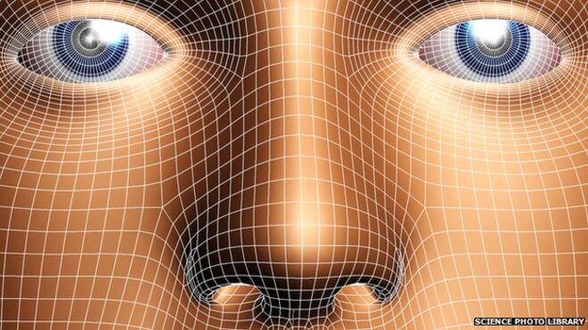
Face recognition technology has become a common thing nowadays as it has now reached even that smartphone you are currently holding in your hand. This technology is a revolutionary one and apart from residing in your smartphone does a lot of work for government agencies as far as identification and surveillance is concerned. Face recognition technology involves the comparison of two photos clicked in well-lit environment.

_84569739_facialrecognitionsciencephotolibrary

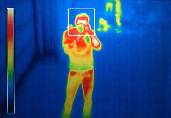
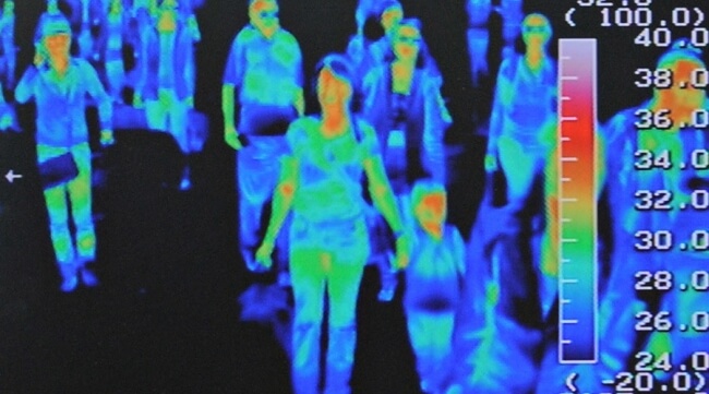
But now, Computer scientists Saquib Sarfraz and Rainer Stiefelhagen from the Karlsruhe Institute of Technology, Germany, have taken this technology to another new level. Using this technology, now you can identify faces even in the dark using a person’s thermal signature. The system analyzes dozens of images of a person’s face and then compares these to dozens of images taken in the daylight using a computer program.

thermal-face

The technology still needs a bit of refining because the thermal image of a person can change or fluctuate based on weather conditions or on the level of physical activity the person is involved in (thermal image of a person leaving a gym after a strenuous workout will be different from one that was taken in normal strain free environment).

But whenever this refining is done, this advancement in technology will surely take the law enforcement agencies ahead in the field of identification and surveillance.

[adinserter block=”7″]

Author: Technology Blog

GaN transistors: A new way of cutting down on energy losses

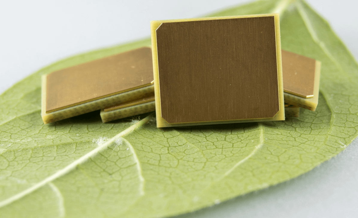
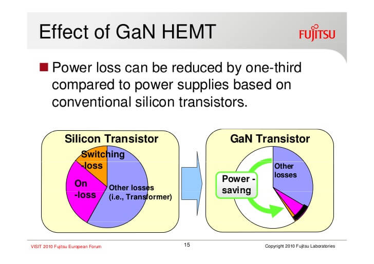
It is a well known fact that most of the electronics systems rely on silicon transistors that in order to regulate voltage switch on and off but due to speed and resistance constraints, waste energy as heat. To offer a solution to this problem, Massachusetts Institute of Technology spin out Cambridge Electronics Inc (CEI) has announced a line of GaN transistors and power electronic circuits that promise to cut energy usage in data centres, electric cars, and consumer devices by 10 to 20 percent worldwide by 2025. These GaN transistors have at least one-tenth the resistance of such silicon based transistors and hence have much greater energy efficiency.

visualization-in-the-design-and-operation-of-efficient-data-centers-15-728

All these benefits were a great thing to start with but due to safety drawbacks and expensive manufacturing methods the GaN transistors could not make it to the market. The researchers have now managed to address these issues. Power transistors are designed to flow high currents when on, and to block high voltages when off but GaN transistors always allows a flow of current by default. By modifying the structure, the researchers developed GaN transistors that were ‘normally off’. To drop manufacturing costs, the researchers developed new fabrication technologies which involved switching out gold metals used in manufacturing GaN devices for metals that were compatible with silicon fabrication, and developing ways to deposit GaN on large wafers used by silicon foundries. CEI co-founder Tomas Palacios, an MIT associate professor who co-invented the technology said: “We always talk about GaN as gallium and nitrogen, but you can modify the basic GaN material, add impurities and other elements, to change its properties.”

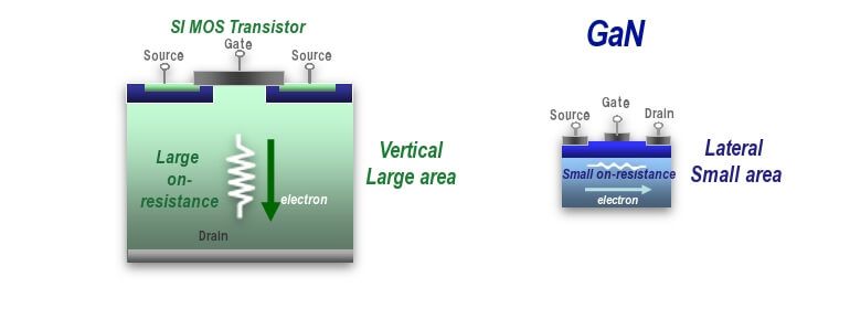
Panasonic_GaN1_e

These new and improved GaN transistors are being used by the CEI in various applications, for ex. developing laptop adaptors that are approximately 1.5 cubic inches in volume and that is the smallest adaptor ever made. Other application of this transistor is in imparting better power electronics for data centres run by Google, Amazon, Facebook, and other companies (which currently utilise 2 percent of electricity in the US), to power the cloud. Also, these transistors may replace the silicon-based power electronic in electric cars which is hoped to boost the energy efficiency of these cars by making them lighter, cheaper and capable of driving long distances.

[adinserter block=”7″]

Author: Technology Blog

Verified by ExactMetrics